Photolithography PCB Fab: Difference between revisions
From HacDC Wiki
No edit summary |
No edit summary |
||
| Line 14: | Line 14: | ||
# UV exposure. Sunlight or high-brightness CFL bulbs can expose the photoresist in ~30 minutes. | # UV exposure. Sunlight or high-brightness CFL bulbs can expose the photoresist in ~30 minutes. | ||
# Development. Use a foam brush with the appropriate developer solution from the chemicals shelf. | # Development. Use a foam brush with the appropriate developer solution from the chemicals shelf. | ||
# Etching. | # Etching. Recommend a sponge with ferric chloride to remove exposed copper. This is quicker and less wasteful than the "bath" process. | ||
# Striping. Sodium hydroxide completely removes photoresist. May need additional UV exposure. | # Striping. Sodium hydroxide completely removes photoresist. May need additional UV exposure. | ||
# Solder mask. Optional. Laminate two dry film photoresist sheets onto the PCB, apply photomask, expose, and develop. Alternatively, laser cut a negative solder mask from blue tape, and apply high-temperature spraypaint. | # Solder mask. Optional. Laminate two dry film photoresist sheets onto the PCB, apply photomask, expose, and develop. Alternatively, laser cut a negative solder mask from blue tape, and apply high-temperature spraypaint. | ||
| Line 50: | Line 50: | ||
http://www.instructables.com/id/Killer-PCBs/ | http://www.instructables.com/id/Killer-PCBs/ | ||
http://www.mgchemicals.com/downloads/pdf/negativePrototyping.pdf | http://www.mgchemicals.com/downloads/pdf/negativePrototyping.pdf | ||
http://www.instructables.com/id/Sponge-Ferric-Chloride-Method-Etch-Circuit-Bo/ | |||
Revision as of 21:42, 27 January 2014
When the 10mil isolation paths offered by CNC Milling are insufficient, photolithography becomes the PCB fabrication method of choice.
PCB Design
Recommend gEDA. Project template with CNC Mill and gerber export scripts available on github.
Process
Simple, consisting of:
- Photosensitive copper clad board. If not already available, more can be made by laminating dry film photoresist to bare copper clad board.
- Via/hole drilling, outline milling, etc. Best done automatically on CNC mill.
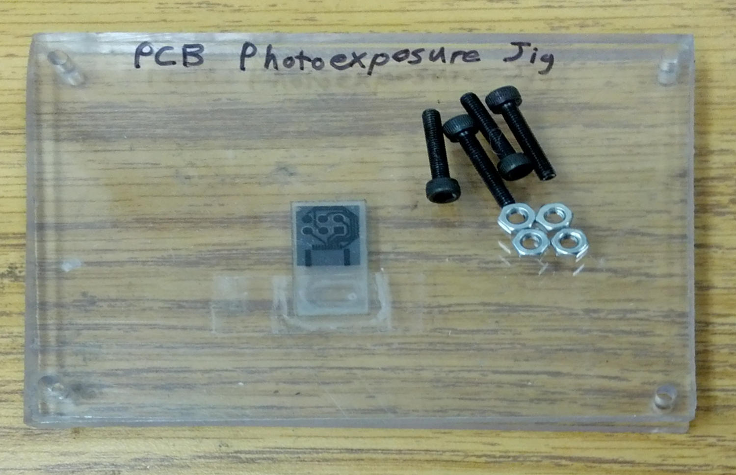
- Photomask. Printed on transparencies at high-resolution. Some laser printers may require double layer photomasks. Alternatively, <445nm lasers may be able to selectively expose the photoresist.
- UV exposure. Sunlight or high-brightness CFL bulbs can expose the photoresist in ~30 minutes.
- Development. Use a foam brush with the appropriate developer solution from the chemicals shelf.
- Etching. Recommend a sponge with ferric chloride to remove exposed copper. This is quicker and less wasteful than the "bath" process.
- Striping. Sodium hydroxide completely removes photoresist. May need additional UV exposure.
- Solder mask. Optional. Laminate two dry film photoresist sheets onto the PCB, apply photomask, expose, and develop. Alternatively, laser cut a negative solder mask from blue tape, and apply high-temperature spraypaint.
Assembly
For large boards with hundreds of components, reflow can be quicker than manual soldering.
- Laser cut solder paste stencil from blue tape. Apply stencil to PCB.
- Add smooth, paper thin layer of solder paste with a razor.
- Remove stencil.
- Place components on the appropriate pads.
- Carefully melt the solder with the hot-air reflow tool. Hold the hot-air tool close to the components at 400C and maximum airflow, watch carefully, and progressively move the tool across the board as solder melts.
Resources
HacDC has the requisite resources:
- Laser printer.
- Transparencies.
- Photosensitive copper clad board.
- Dry film photoresist.
- Various photodeveloper chemicals.
- Copper dissolving etchant.
- CNC Mill.
Demo
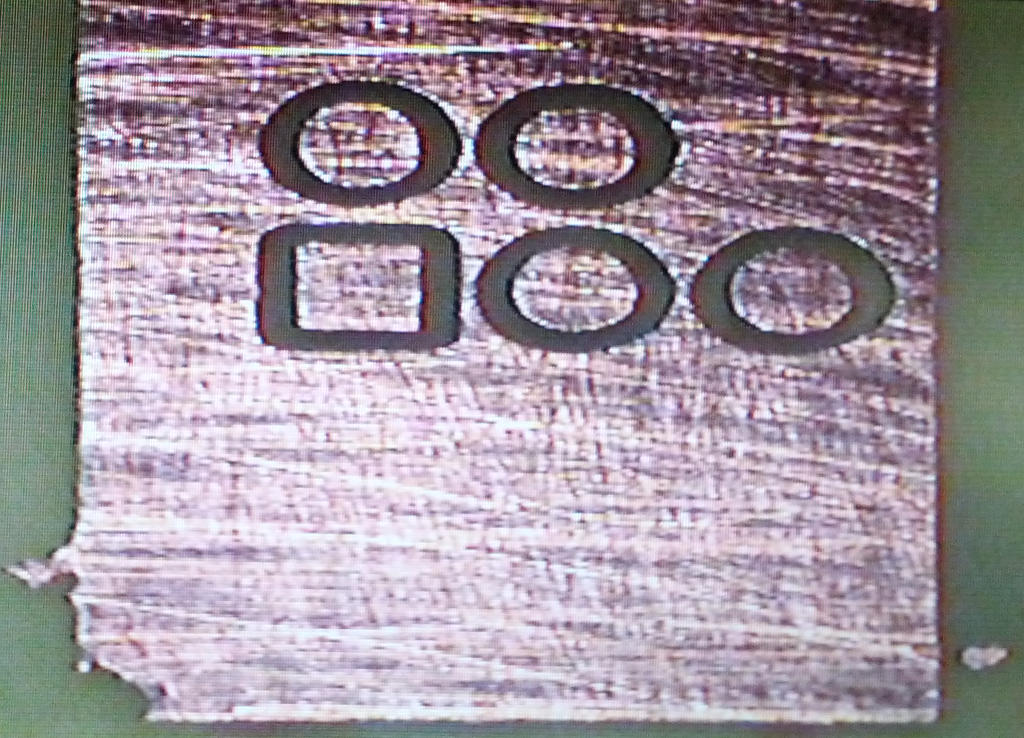
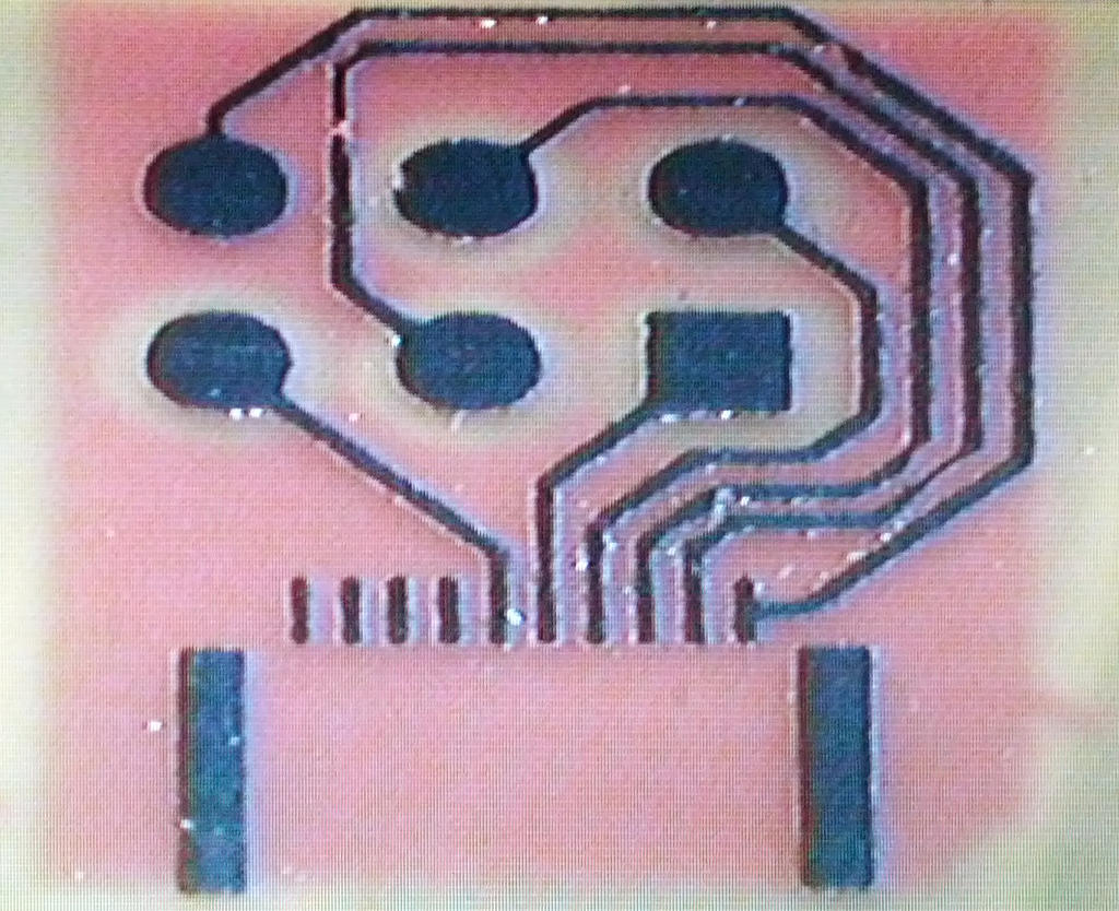
Chemically developed and etched PCB. Photomask remaining.
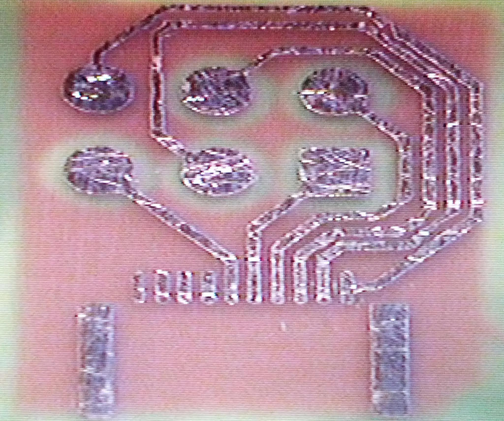
Photomask stripped, bare copper PCB electrically tested.
Reference
http://www.instructables.com/id/Killer-PCBs/ http://www.mgchemicals.com/downloads/pdf/negativePrototyping.pdf http://www.instructables.com/id/Sponge-Ferric-Chloride-Method-Etch-Circuit-Bo/
