Photolithography PCB Fab: Difference between revisions
From HacDC Wiki
No edit summary |
|||
| Line 90: | Line 90: | ||
* PCB processing spray tanks for developing and etching. Expected to improve quality and ease of use, allowing higher yields and more attempts as necessary. | * PCB processing spray tanks for developing and etching. Expected to improve quality and ease of use, allowing higher yields and more attempts as necessary. | ||
* CircuitWriter repair pen to repair scratched or undercut traces. | * CircuitWriter repair pen to repair scratched or undercut traces. | ||
* Conductive ink or rivet (http://www.megauk.com/through_hole_rivets.php) through-hole connections. | * Conductive ink or rivet (http://www.megauk.com/through_hole_rivets.php) through-hole connections. Apparently, the rivets can be used without the expensive punch tool (http://www.electricstuff.co.uk/pcbs.html). | ||
==Full-Scale Process== | ==Full-Scale Process== | ||
Revision as of 23:42, 29 June 2014
When the 10mil isolation paths offered by CNC Milling are insufficient, photolithography becomes the PCB fabrication method of choice.
Large Boards
For large boards, note the following:
- Foam backing will be needed to press the PCB evenly against a photomask. Otherwise, acrylic (and similar) frames may bubble under pressure, allowing the photomask to 'pop-up' in the middle.
- During chemical processing, alternate between photodeveloper and etchant. Proceed with etchant only when all exposed regions are changing color. Otherwise, problems with ultrathin photoresist residue may remain.
- Avoid placing UV light sources in extreme proximity to the board. Doing so may unevenly expose some regions.
PCB Design
Recommend gEDA. Project template with CNC Mill and gerber export scripts available on github. Photolithography scripts are specifically provided at the HacDCPhotolitho github repository.
Design Rules
Recommend at least the following tolerances:
- 6 mil (0.15mm) feature size (traces and spacing)
- 34 mil (0.85mm) hole size with 8 mil (0.21mm) annular ring size (50mil/1.25mm outside diameter) - fits most through-hole components, standardization on one size obviates manual milling bit swapping
- 25 mil minimum hole size - tested for milldrilling
For comparison, oshpark offers:
The minimum specs for 2 layer orders are 6 mil traces with 6 mil spacing, and 13 mil drills with 7 mil annular rings.
Recommend most traces be kept to 10mil width, especially long traces. Note slightly better resolution is routinely feasible with practice.
Process
Simple, consisting of:
- Photosensitive copper clad board. If not already available, more can be made by laminating dry film photoresist to bare copper clad board.
- Via/hole drilling, outline milling, etc. Best done automatically on CNC mill. Please be careful to terminate outline cutting once complete, do not allow the endmill to bind.
- Photomask. Printed on transparencies at high-resolution. Inkjet printers, >600dpi, do well, given true inkjet transparencies. Some laser printers may require double layer photomasks. Alternatively, <445nm lasers may be able to selectively expose the photoresist.
- UV exposure. Sunlight or high-brightness CFL bulbs can expose the photoresist in ~5-30 minutes. EEPROM eraser boxes with timers are best. Even exposure is critical, and timing is critical for lower-contrast photomasks.
- Development. Use a foam brush with the appropriate developer solution from the chemicals shelf. Alternatively, a warm bath can quickly provide better consistency across large boards, particularly if photodeveloper includes silicate.
- Etching. Recommend a sponge with ferric chloride to remove exposed copper. This is quicker and less wasteful than the "bath" process.
- Carefully repeat above two steps as necessary to isolate all traces.
- Striping. Sodium hydroxide completely removes photoresist. May need additional UV exposure.
- Solder mask. Optional. Laminate two dry film photoresist sheets onto the PCB, apply photomask, expose, and develop. Alternatively, laser cut a negative solder mask from blue tape, and apply high-temperature spraypaint.
Assembly
For large boards with hundreds of components, reflow can be quicker than manual soldering.
- Laser cut solder paste stencil from blue tape. Apply stencil to PCB.
- Add smooth, paper thin layer of solder paste with a razor.
- Remove stencil.
- Place components on the appropriate pads.
- Carefully melt the solder with the hot-air reflow tool. Hold the hot-air tool close to the components at 400C and maximum airflow, watch carefully, and progressively move the tool across the board as solder melts.
Note that this process is somewhat incompatible with hand-soldered vias.
Resources
HacDC has the requisite resources:
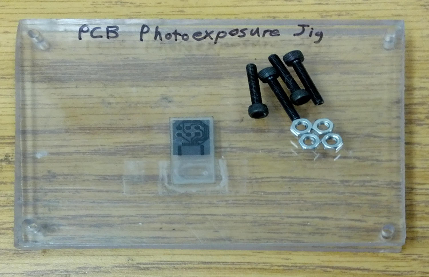
- Modified EEPROM exposure box including timer, germicidal lamp, foam backing, and laser-cut acrylic PCB/photomask holding jig.
- Standalone polycarbonate and acrylic PCB/photomask holding jigs, for use with alternative light sources.
- Laser printer (Phaser740, use dual layer transparency masks, monochrome only, color causes streaks).
- Transparencies.
- Positive photosensitive copper clad board (typically including 590-660).
- Negative photosensitive copper clad board.
- Negative dry film photoresist.
- Bare copper clad board, various types and thicknesses.
- Various photodeveloper chemicals. Use the positive developer solution and foam brush for positive resists, sodium carbonate (washing soda) for negative resists.
- Lots of copper dissolving etchant, various types, some good, some bad.
- CNC Mill.
- A heated and bubbled etchant bath has been constructed by mirage335. While reasonably quick (~15 minutes) and consistent, this is not recommended, as components degrade quickly, and the resulting acid vapor is extremely harsh.
Demo
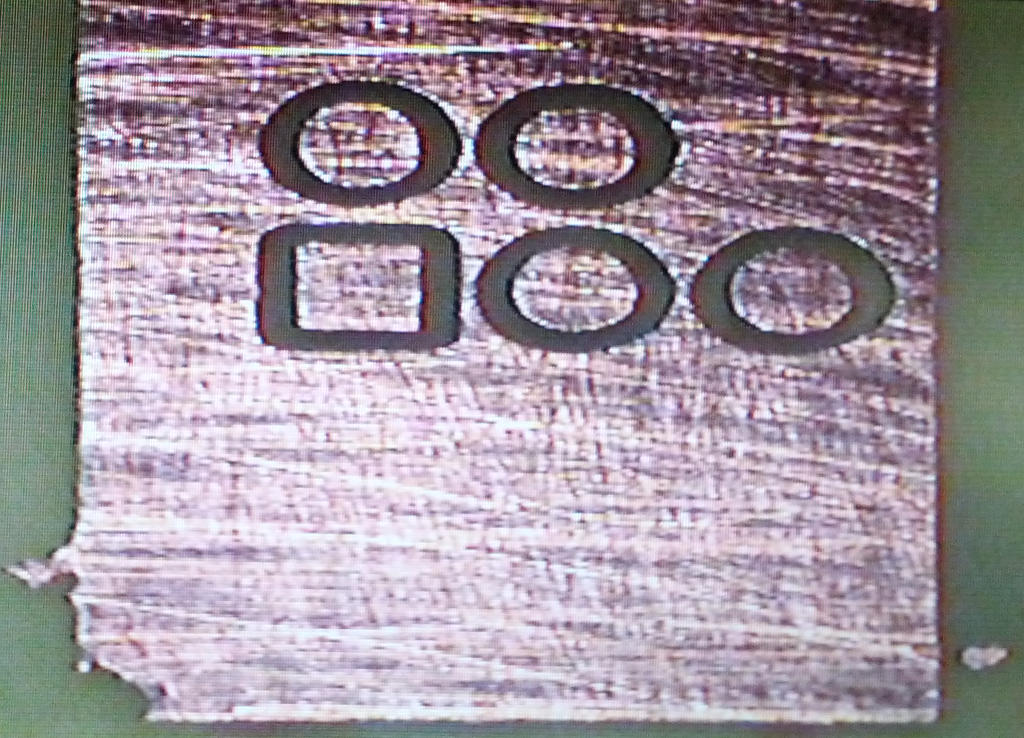
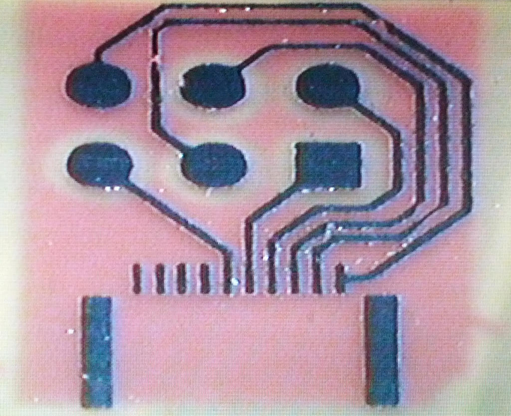
Chemically developed and etched PCB. Photoresist remaining.
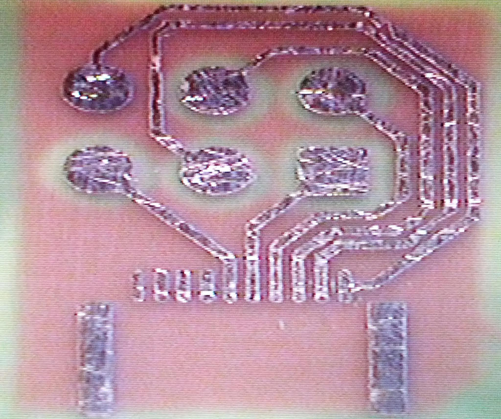
Photoresist stripped, bare copper PCB electrically tested.
Reference
http://www.instructables.com/id/Killer-PCBs/ http://www.mgchemicals.com/downloads/pdf/negativePrototyping.pdf http://www.instructables.com/id/Sponge-Ferric-Chloride-Method-Etch-Circuit-Bo/
Credit
Many thanks to:
- Dan Barlow
Research Underway
- Better photodeveloper. The MG Chemicals product works reasonably well thus far, but may not include sodium silicate. [Reportedly] RS-Components 690-849 is far superior, allowing development in seconds with lower risks of overdevelopment.
- Alternative photoresist, as reported at [1].
- DLP projector maskless lithography.
- Tracing paper photomasks, as reported at [2].
- PCB processing spray tanks for developing and etching. Expected to improve quality and ease of use, allowing higher yields and more attempts as necessary.
- CircuitWriter repair pen to repair scratched or undercut traces.
- Conductive ink or rivet (http://www.megauk.com/through_hole_rivets.php) through-hole connections. Apparently, the rivets can be used without the expensive punch tool (http://www.electricstuff.co.uk/pcbs.html).
Full-Scale Process
Professional PCB fabs manufacture upwards of dozens of PCBs per hour, with resulting boards ready for rapid soldermask-based PCB assembly. The process is as follows:
- Positive presensitzed board, negative artwork (dark regions cover desired copper).
- UV photoexposure, high contrast, using DLP projection.
- Photodevelopment spray (exposes desired copper).
- Rinse spray.
- Via/hole drilling, if not done already.
- Heated press prepeg bonding (optional, only for >2 layer PCBs).
- Conductive ink coating, to activate through-holes (http://www.thinktink.com/stack/volumes/volvi/condink.htm).
- Spray electroplating (adds copper everywhere, including holes). Requires specialized copper plating solution (http://www.thinktink.com/stack/volumes/voliii/consumbl/cplatmix.htm) .
- Liquid tin plating (simple bath, no spraying) covers everything with tin, which resists etchant.
- Photoresist stripping with concentrated sodium hydroxide.
- Etching spray removes bare copper, leaves previously tinplated surfaces unharmed.
- Rinse spray.
- Tin stripping spray (http://www.alliedelec.com/search/productdetail.aspx?SKU=70125740) leaves bare copper.
Efforts are underway to implement required DLP projection and spray tank equipment. Total system cost is expected to be ~$1.5k.
